Electrical Transport
with RuCl₃
Overview
Schottky barriers at graphene–TMD interfaces introduce contact resistance that obscures the intrinsic transport properties of WS₂ and MoSe₂. By depositing multilayer RuCl₃ on graphene contacts, its exceptionally large work function drives interlayer charge transfer — hole-doping graphene to high carrier densities and converting the junction from Schottky to metal-like, enabling accurate electrical transport measurements.
Device Stack
Fabrication
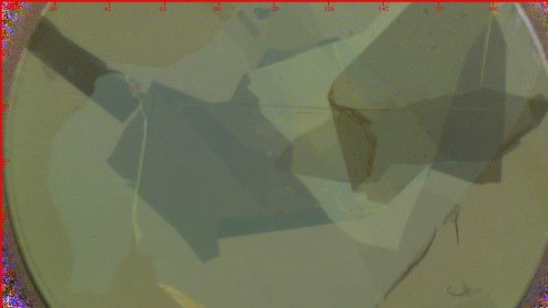
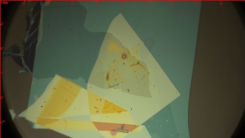
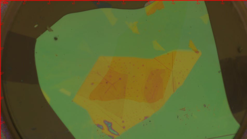
Three device generations were fabricated. Initial dual-gate stacks with twisted WS₂ did not perform as expected due to heterostructure complexity. A simplified single-gate MoSe₂ device was successfully fabricated and measured.
Results
Two-terminal resistance was measured at 76 K as a function of source–drain voltage across three back-gate voltages using a liquid nitrogen dewar.
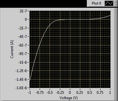
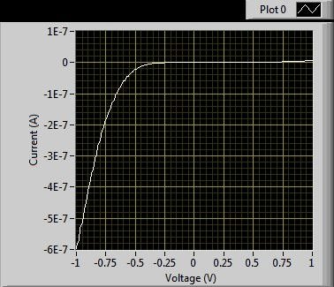
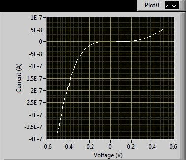
Progressive linearization — I–V curves become more symmetric as gate voltage increases, consistent with carrier-density screening of the Schottky barrier.
Residual barrier — Pronounced nonlinearity persists near Vsp = 0 even at 10 V, indicating the Schottky barrier was not fully eliminated.
High contact resistance — ~1 MΩ at Vsp = 1 V, compared to <10⁵ Ω for fully ohmic graphene contacts on WS₂ after annealing (Ovchinnikov et al., ACS Nano 2014).
Dielectric limitation — The 30 nm hBN gate dielectric screens the electric field, restricting achievable carrier density at 10 V.
Next Steps
Thinner Gate Dielectric
Replace 30 nm hBN with 10 nm — tripling the electric field at the same gate voltage to access higher carrier densities.
VTI Cryostat to 2 K
Low-temperature measurements suppress thermal broadening and more clearly resolve intrinsic contact properties via tunneling diagnostics.
Metal Contacts + RuCl₃
Au or Ti/Au contacts with RuCl₃ on top to isolate whether the barrier originates at the graphene–TMD interface.
Four-Terminal Measurements
Decouple contact resistance from channel resistance, benchmarking against strict linear I–V across ±2 V at all gate voltages.